My log of trying to build a CPU/computer using 7400 series TTL logic ICs. The older entries are at the bottom of the page so start reading from there. :)
A short update to include the design, decoder updates and unit test code to include externally generated IRQs. When EXTWANTIRQ goes from hi to lo, a negative edge, it is latched and then tested with the I (interrupt disable) ST flag when the state kD5IRQStateLE is used. If interrupts are not disabled (i.e. the processor is not running in the IRQ operating level) this then causes states opStartIRQ and opStartIRQ2 to be executed which stack ST, the return address and set the interrupt disable flag. The instructions interrupt related instructions SEI, CLI and RTI have also been added. Unfortunately an extra decoder is required for the extra logic control so this will mean a bigger board layout is needed, once it has been updated.
The parts for the alphanumeric LCD arrived today so out came the soldering iron again. This time here is a video of the CPU running some quick and dirty test code.
This is running at 2 MHz and the pause between it printing "Min" and "Max" on the display is 20,000 cycles of a "dex/bne" loop. The same test also runs at 15625 Hz (4 MHz / 128 on the clock divider) and allows the individual characters to be seen being sent to the display.
The next stage is to attach some sort of colour graphics display.
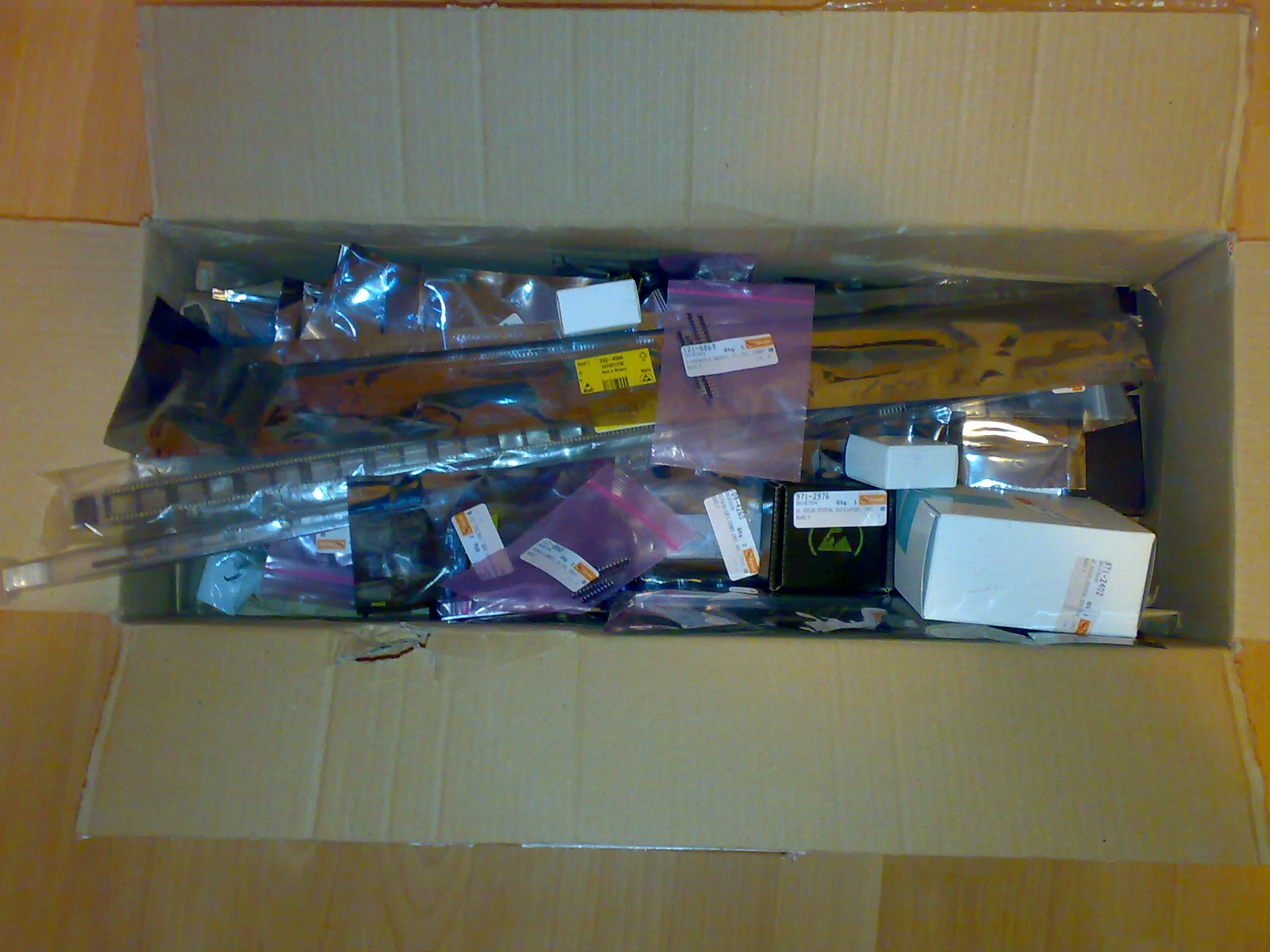
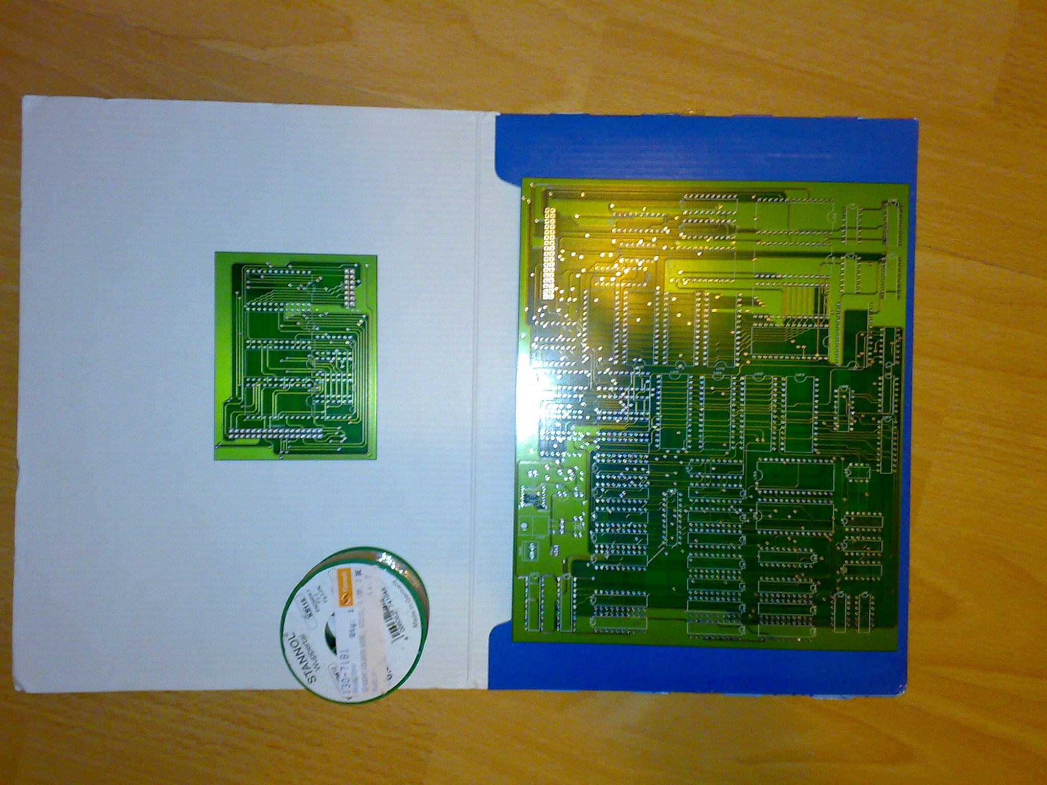
All the parts and circuit boards arrived last week so this weekend was the time to assemble it all. I accidentally damaged the expansion board while unpacking, it flew out of the packet in a bid for freedom, onto the desk and then the floor, so I have ordered a replacement. I took this opportunity to improve on the design by adding a different LCD connector socket, a debug header block and the ability to choose the operating clock frequency by a clock divider using a pair of 74161s.
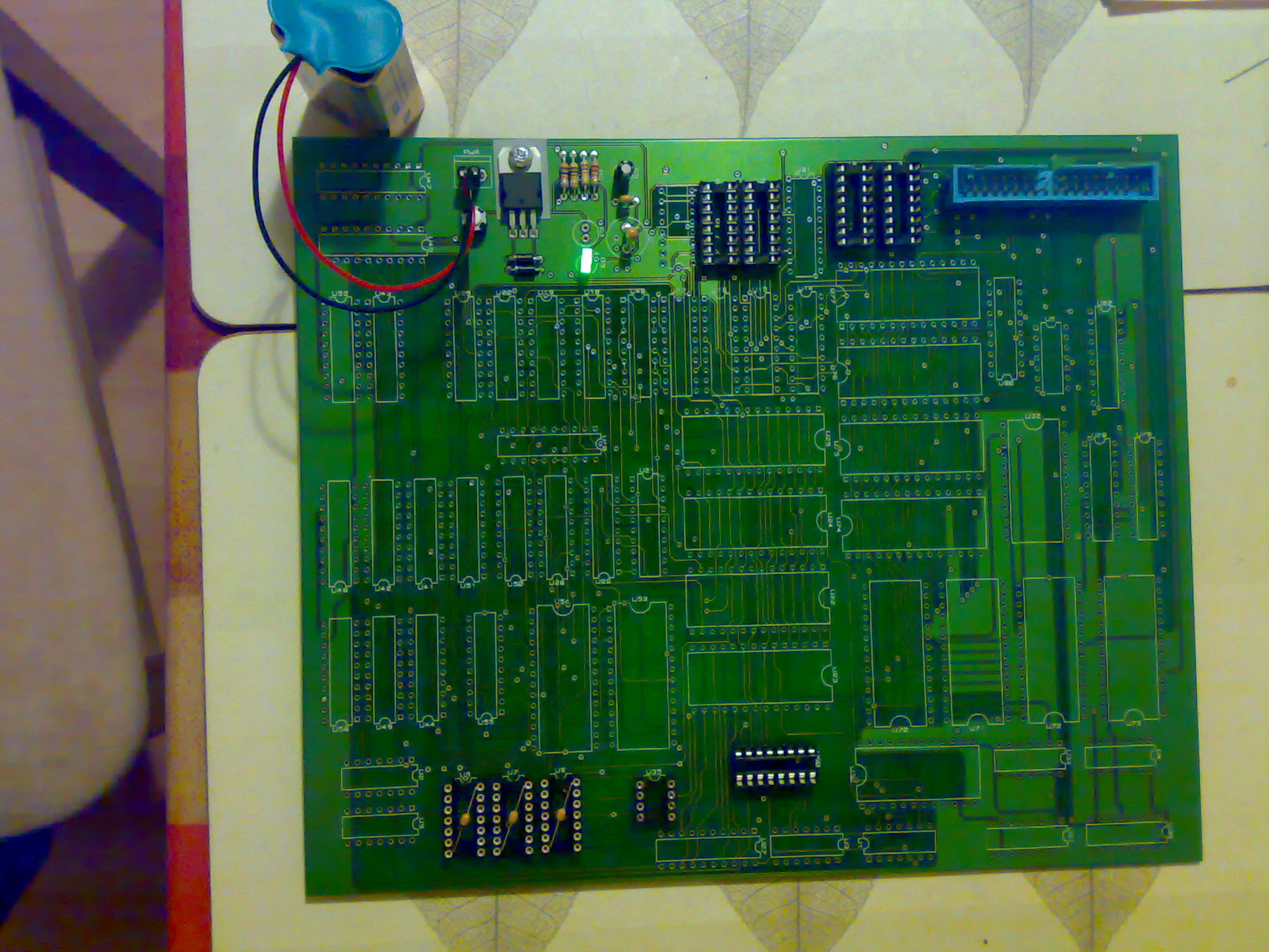
The first stage was to sparsely populate the main board and test the power circuit could supply power without shorting anywhere. The bright green LED can be seen just below the resistors at the top of the board.
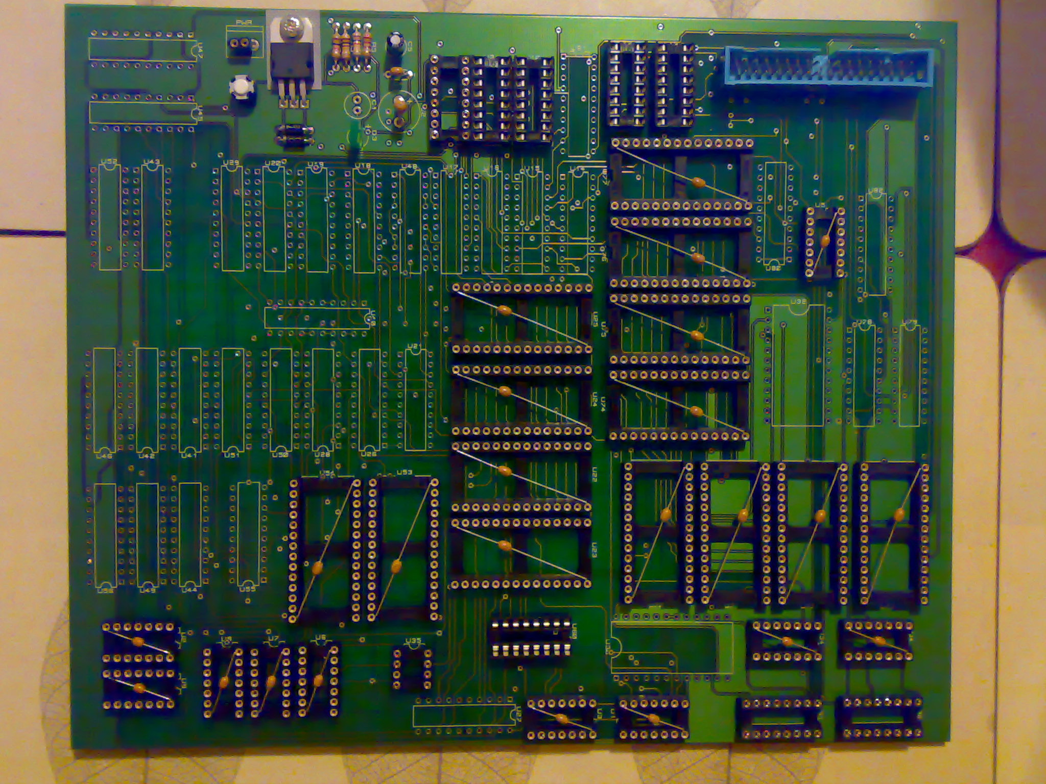
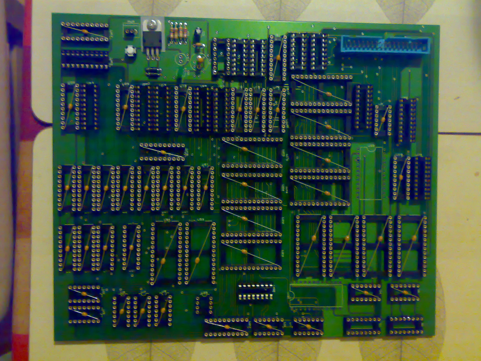
Next, more IC sockets are added over the course of the weekend. Notice how most of the sockets have decoupling capacitors built into them, these are slightly more expensive than normal sockets but do help to smooth out power fluctuations.
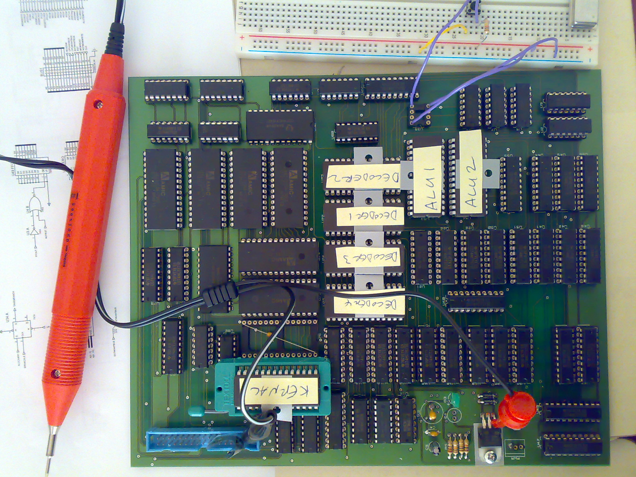
Then came the stage of adding all the ICs and running tests with a logic probe. As you can see I've labelled the EPROMs which also has the handy effect of obscuring their UV erasing windows from the spring sunlight. The kernal EPROM (remember this is C64 kernal land, not the land of kernels) has been mounted in a ZIF socket which is mounted in the decoupling capacitor socket. The BASIC EPROM is left unplugged for these initial tests. I also created a very small minimal program that only exists in the KERNAL EPROM that would be just enough to activate and display a message on the LCD expansion board.
The breadboard is being used to give me a push button so I can single step advance the clock or use a 1MHz oscillator.
Now the moment of truth, switching it on and checking. Initial checks with the voltage probe showed a small issue with one line of the data bus not being active on all connected ICs. This was traced to a connection problem between IC 43 pin 7 and IC 52, a quick wire soldering job later and it was fixed.
Next came the job of manually checking the opBoot process and a few instructions worth of states. This involved using the push button to advance each clock cycle and using the logic probe to check the states of the pins for various important ICs, like the registers, program counter, address storage and ALU results, with the expected results from the Proteus simulation. First run through all seems good so I let the board run for a few seconds with the 1MHz clock tied in. I would then stop the processor at a random point (not much choice with it running at 1MHz) and testing the results of the state with the known values such as opcode, program counter and data bus or register state. After several tests of this nature I'm now confident it is operating roughly as expected. A logic analyser with at least 32 inputs (16 bit address, 8 bit data bus and 8 bit clock counter) would have been an excellent idea and would have saved me poking around the circuit with a logic probe, I must put this on my list of things to acquire.
The last test was to use the breadboard to display the results of the data bus and memory write (to the LCD output) with a few LEDs. This also seemed to work as expected. I am now the proud owner of quickly blinking lights caused by a lot of ICs.
As usual all the source and project files for this update are included.
Next stage will be to assemble the expansion board and hopefully get some text and graphics displayed.
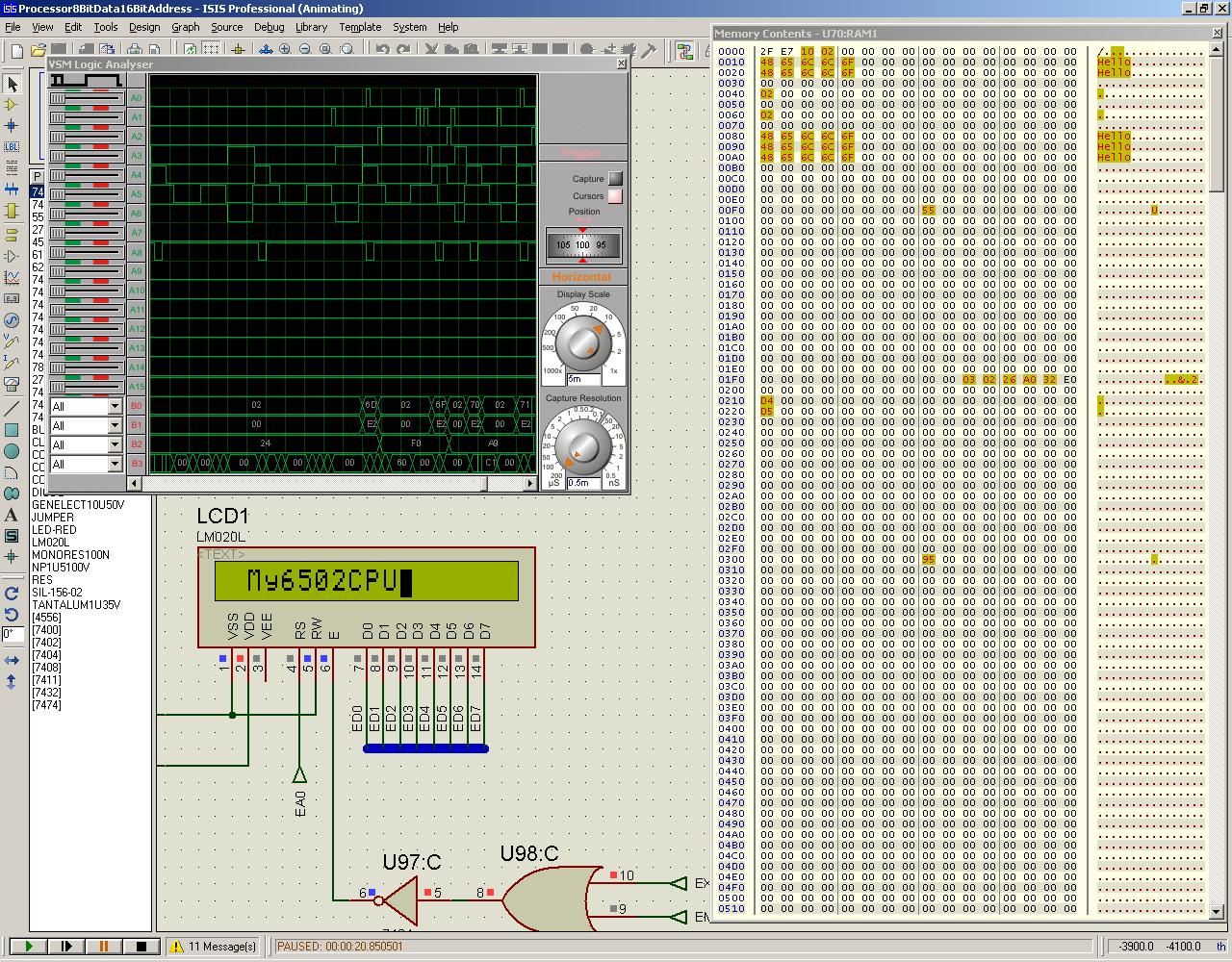
Now the design will allow an external device to be attached via the expansion bus. This bus is tri-stated when it is not being used by the processor which allows an external device to use the bus instead. There are also lines to say when the processor is using the bus, when it wants the bus, the data direction of the bus and strobes for reading or writing memory. One other line (EXTWANTBUS) is designed to be used by whatever is on the expansion bus to signal that it wants to pause the processor and has exclusive access to the bus. When this line is pulled low and the CPU wants to use the bus the CPU will wait until EXTWANTBUS is high again. In the simulation this line is repeatedly alternated to test that the unit test executes correctly with the CPU being paused and unpaused by an imaginary external device, normally this line would be held high or float high thus allowing the CPU to execute. In the screen shot the A5 line is EXTWANTBUS. A4 is CPUHASBUS. A3 is CPUWANTBUS. A6 is CPUCLKACTIVE. As can bee seen on the logic analyser output CPUCLKACTIVE will become low when CPUWANTBUS is high and EXTWANTBUS is low, this pauses the CPU. CPUHASBUS will only become high when EXTWANTBUS is low and if the CPU currently has the bus then the CPU will not pause until the next time CPUWANTBUS happens. This does mean EXTWANTBUS must be signalled, then a wait of one clock cycle must be made before checking CPUHASBUS is low, however on the data bus ECPUHASBUS is the inverse of CPUHASBUS to match the low active state of EXTWANTBUS.
To test this I created an expansion board using which only uses the lines listed on the expansion bus. This uses the "Alphanumeric LCD Display Model (HD44780)" from Proteus and memory maps the device to the C64 external device memory addresses at $de00/$de01. The low bit of the address is used to change the RS line on the LCD display. Adding some code to the unit test to write data to these addresses then sends data bytes to the display which shows the message. The expansion board also has separate memory to emulate the C64 VIC and SID chips and screen colour memory. This screen shot shows the simulated LCD display with the new unit test message.
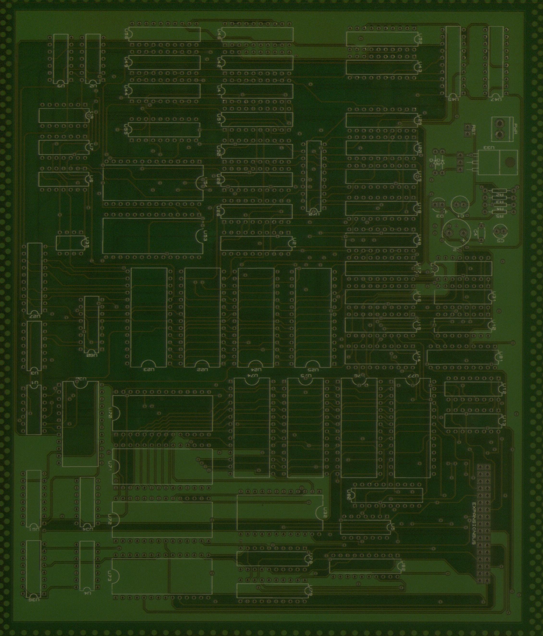
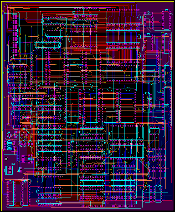
I bit the bullet and upgraded Proteus beyond the basic version so it would handle more than 500 pins in the netlist when exporting to ARES the PCB design package. As can be seen from the new download I tried to split the PCB into four sections each less than 500 pins. This was done but the boards also had to use two layers as this is the limit with the basic version of Proteus and trying to route the design with two layers was possible but meant spreading out the components onto large PCBs which was wasteful and expensive. So I chose to populate one board with the main part of the processor using four layers and the expansion board using 2 layers instead. This screen shot shows the layout of all four layers plus the silk screen.
Then I tidied up the design, made absolutely sure it did exactly what I wanted, created the final layout by tweaking the version Proteus created and let the router do its job, which takes about half an hour. Then the big step of ordering the boards and parts needed to construct this project, which took two parts suppliers and a fair amount of time to source the most suitable components. I have used this company to order the PCBs http://www.pcb-pool.com/ since they are recommended by the makers of Proteus and can accept the layout files this software produces. This company have an online ordering system that allows your PCB order to be merged with other orders to keep costs down and they even allow you to change your order by adding new layout files right up until the point they are ready to start the manufacturing process. Even so, buying the PCBs and components needed to make this project is quite high, but that is the cost of trying to make prototypes. :) All these items will take a few weeks to arrive.
Next step, construction and testing. And pulling hair out, I expect...
I'm a computer programming geek. It's what I do as my hobby and my job, having a job as a hobby is a blessing and probably a curse to some who know my ability to talk at length about this subject. I've been programming for as long as I can remember. Just before Christmas 2007 I encountered a website about designing a video game system which was recommended during a discussion about retro computing. Many years ago I cut my programming teeth on a machine called the Commodore 64. This machine was really powerful for its time having 64KB of RAM and custom video and sound chips. The video chip especially always fascinated me because according to the specs it could only display eight sprites with the usual compliment of character and bitmap based screen modes. But using machine code with careful timing techniques it was possible to get the chip to display much more than the specs said it could. For example it is possible to display many times the standard eight sprites, stretch the sprites much more than the original x2 and also display many more colours for each character cell. These raster and timing effects are possible because the chip internals used timers and latches which could be tricked into accessing data more frequently than normal, for example. Why? Well the gate design of the chip just allowed these effects as part of the logical operation. So as you can see the subject of electronics always interested me from a programming point of view because programming in machine code is effectively one step away from shifting around tiny bits of electronic information in such a way to get a computer to do something useful.
Anyway back to the video game system design site. The site sells kits with components and boards to solder together. It also sells a really thick book of around 900 pages called "The Black Art of Video Game Console Design". After having a quick read through the PDF version I knew it looked like it would teach me something useful, so I bought a copy along with the small Pico Edition kit. The joy of getting all these little components, soldering them onto a board and then seeing Pacman appear on my TV is very much like the "Eureka!" feeling of solving a programming problem. I was hooked, completely, utterly and totally.
As it was now Christmas I used this spare time to digest the entire contents of the book. It starts off explaining analogue components, then getting onto digital components like the transistor. Most of this knowledge was a refresher course of my Physics classes from 1990, Mr. Telfer my physics teacher would be proud if he knew. Then the book progresses onto digital logic (TTL) such as what makes an adder, how latches work and so on. It also then describes processor design as state machines. These concepts are easily understood at a software level since they are encountered in normal day-to-day programming. However this was the point where there was another Eureka moment. The book recommends some electronic simulation software called Proteus VSM. This software allows circuits to be created as a schematic and importantly allows these circuits to be simulated without building them out of physical components. My brain was fizzing with ideas from the book because being able to manipulate and store bits is just one step away from machine code programming.
The demonstration version of Proteus does not allow saving, but even so some of my first simple logic circuits were designed that would simulate NAND and NOT calculations, then using existing TTL blocks of as NAND gates an adder was produced that would add with carry two 4 bit numbers. After this evaluation I was even more hooked than before and so I bought the base version which allows files to be saved. Very quickly larger circuits were created and simulated that would allow data to be written and read from RAM. Then I bit the bullet and decided to try to create something using this knowledge, the logical choice would be a processor made from logic gates, or rather a processor made from 74 series TTL chips as these contain small groups of logic gates to do common tasks.
My initial design grouped together some 8 bit latches for registers, a simple ALU and program counter. The program itself was read from memory by the program counter, the opcode would trigger an ALU operation and the result would be stored to another register. The program counter was 8 bits so the program was really small. Getting it to work was a learning experience, for example memory chips like to have correct set-up times and enabled/disabled at the correct time with respect to their address lines otherwise they can drive outputs when disabled and cause logic contentions. Luckily the simulation software allows a breakpoint to be set for logic contentions making the job of debugging a lot easier and I cannot praise the simulation software highly enough, it is extremely powerful. Eventually the simulation worked, in as far as it was possible to write a program to perform calculations in order and generate a result at the end. This took slightly less than 700 connections between TTL chip pins and other supporting components. A good proof of concept for my new knowledge. However the design is not that useful in the real world, that is to say each opcode is a fixed length of time, not that complex and doesn't have branches.
Now it was time to try a more advanced project for something that would be more useful. I like to think I know the 6502/6510 CPU really well because it was used in the Commodore 64 and other home computers. It also has a relatively simple to understand opcode set, 8 bit registers and a 16 bit address bus. But I also wanted something a little more generic so I designed a processor with seven 8 bit general purpose registers, 8 bit status, 16 bit address bus, a more powerful ALU and the opcode decoder. The idea being that some of the general purpose registers could be used for the stack pointer or to allow more flexible addressing modes such as taking an address and adding a register offset, or indirect zero page addressing. The opcode decoder is the heart of the chip which is a lookup table that allows the inner blocks of the processor to switch on and off at the correct times according to the clock, this is called microcode. Without a decoder then it is possible to do this with large logic gate arrays or to have the program in memory to describe what sections to turn on and off, however a decoder allows an opcode to have many complex steps while allowing the processor to be more easily expanded. Another advantage is that hardware can be changed but the opcodes remaining functionally the same with only a change in the microcode needed. This is a lot like reusing functional blocks of code in software programming. The ALU is basically a giant lookup table which takes two 8 bit registers, status flags and an ALU operation. A quick calculation for two 8 bit registers, plus 2 bits for input flags (carry, decimal mode) and 4 bits for the ALU operation brings the total to 22 bits. This is a huge lookup table to store on a single chip. It's possible but not that practical. So splitting the operation into two 4 bit halves reduces the pin count but also means cascading two lookup tables together to generate an 8 bit result plus the status flags.
Now fast forward to the end of February, once the circuit was designed all that was needed was to test it. First of all I created a very simple opcode set that would test very simple operations such as: Fetch memory to R0, fetch memory to R1, add r0 and r1 and store in r2. This allowed me to test by hand the various operating paths of the processor by inspection of the memory and register latches. This also allowed me to debug the hardware and find odd logic issues, for example incrementing the program counter when at the same time fetching the next opcode from memory and resetting the clock cycle counter would cause the processor the endlessly cycle around the memory instead of operating correctly. So basically the hardware has some states that produce undefined results, this was to be expected since electronic signal propagation does take a finite amount of time to complete. I could have designed many more of my own opcodes however this would have meant creating a proper assembler toolchain. Instead I started to emulate 6502 opcodes instead since there are already many bug tested assemblers available.
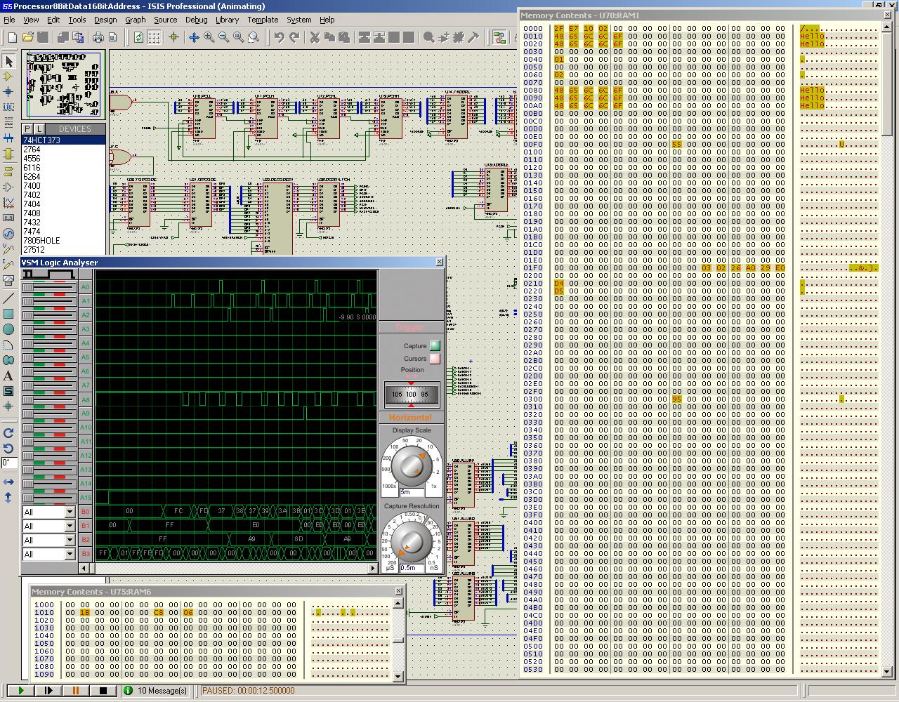
This download link contains all of the source code, Proteus schematic and pre-built binary files needed to demonstrate the working processor. As can be seen from the schematic file "Processor8BitData16BitAddress.DSN" the processor memory is configured to have RAM and ROM areas similar to the Commodore 64. This is by design to allow the normal Commodore 64 ROMs to be used is more complete tests and in fact with minimal "kernal patches" (in C64 land the kernel was called the kernal) detailed in main.cpp the processor will boot to the BASIC start screen. The two asm source files are actually unit test replacements to allow simpler testing of individual opcodes. By using some code to generate expected memory stores and calculations then using different code to generate the same result in a different way or test results it is possible to debug the hardware. These unit test ROMs were developed using a real Commodore 64 emulator to bug test them and then the processor itself was bug tested. The opcode $02 is used to generate a hardware breakpoint in the simulation to allow undefined software operations to be trapped. The files "main.cpp" and "OpCode.cpp" define functional reusable logic blocks and the opcodes for the ALU and decoder lookup tables. Running the processor at 1000Hz one full unit test cycle of the simulation takes approximately 16 seconds on a fast PC. Pausing the simulation and viewing the contents of RAM1 (or RAM6 at offset $1000) will show the memory being changed as the code executes. This is quite slow except remember that real TTL hardware should run at speeds of about 100,000 Hz or more so the unit test would take a much shorter amount of time. Running the real Commodore 64 ROMs with patches takes about thirty minutes to get to the "READY." prompt and this can be seen in the contents of RAM1 at offset $0400, the default screen memory location on a real Commodore 64.
This screenshot shows the processor paused while running the unit test. The memory changed is highlighted and the logic analyser shows the address bus, opcode and data bus values. The processor can be seen to start executing the opcode $ff which bootstraps the processor to read into the program counter from the reset vector at $fffc/$fffd. The opcodes $a9 and $8d are then executed which correspond to the "Start" entry point in "KernalROM.asm".
There are numerous things to improve in this design. For example it doesn't support IRQs/NMIs or being able to pause the processor and tri-state the address and data bus. It is also not cycle exact compared to the real 6502. This means that it isn't possible, as it is, to interface the processor with the Commodore 64 VIC video chip for example. But these of course were not the original design goals. I would definitely take the time to re-engineer this project using edge triggered latches (74374s) instead of the 74373s as this would make timing of the memory access much easier.